Linear Voltage Regulator
Aug 2024—Sept 2024
Student Design Team Project
Skills and Technologies:
Altium, circuits
- Designed a 2-layer linear voltage regulator PCB to drop down 5V to 3V3 for use with a UAV, powering onboard electronics
- Used an LDO integrated circuit, input and output capcitors, and feedback resistors to maintain steady voltage supply
- Included status LEDs to indicate if correct voltage is being supplied and outputted
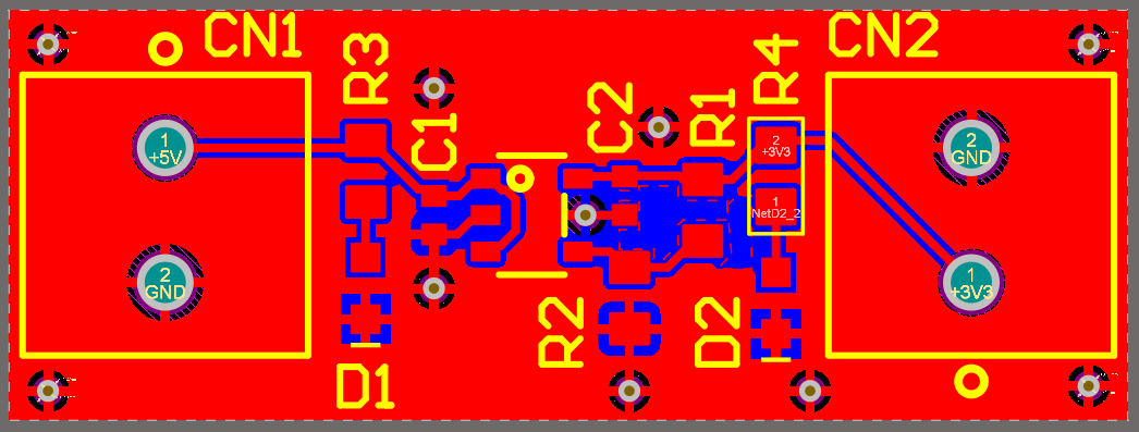
I completed this project to learn more about PCB design and challenge myself to explore another area of engineering. This was my first PCB I have designed and I am really intrigued and wanting to push myself to design another more complicated one that will include embedded programming. Below are images of the shcematic and PCB layout. After receiving feedback from more experienced students, some things I would adjust are ensuring there are no accdiental antennas from the ground pour and adding more vias ensuring better ground connection. I would also try to use board space more efficiently as I feel there is a lot of extra space.

Figure 1: Schematic of the PCB

Figure 2: Layout of components

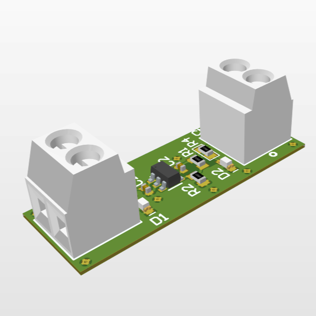
Figure 3: 3D image of PCB